- 您现在的位置:买卖IC网 > Sheet目录1991 > CS43L22-CNZR (Cirrus Logic Inc)IC DAC W/HDPN & SPKR AMPS 40-QFN
DS792F2
27
CS43L22
Confidential Draft
3/4/10
4.5.1
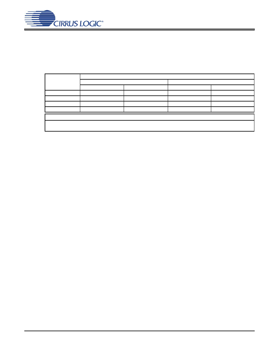
Mono Speaker Output Configuration
The CS43L22 accommodates a stereo as well as a mono speaker output configuration. In mono mode
the output drivers of each channel are connected in parallel to deliver maximum power to a 4 ohm speak-
er. Refer to the table below for pin mapping in mono configuration.
4.5.2
VP Battery Compensation
The CS43L22 provides the option to maintain a desired power output level, independent of the VP supply.
When enabled, this feature works by monitoring the voltage on the VP supply and reducing the attenua-
tion on the speaker outputs when VP voltage levels fall.
Note: The internal ADC that monitors the VP supply operates from the VA supply. Calculations are based
on typical VA levels of 1.8 V and 2.5 V using the VPREF bits.
4.5.2.1
Maintaining a Desired Output Level
Using SPKxVOL, the speaker output level must first be attenuated by the decibel equivalent of the expect-
ed VP supply range (MAX relative to MIN). The CS43L22 then gradually reduces the attenuation as the
VP supply drops from its maximum level, maintaining a nearly constant power output.
Compensation Example 1 (VP Battery supply ranges from 4.5 V to 3.0 V)
1. Set speaker attenuation (SPKxVOL) to -3.5 dB. The VP supply changes ~3.5 dB.
2. Set the reference VP supply (VPREF) to 4.5 V.
3. Enable battery compensation (BATTCMP).
The CS43L22 automatically adjusts the output level as the battery discharges.
Compensation Example 2 (VP Battery supply ranges from 5.0 V to 1.6 V)
1. Set speaker attenuation (SPKxVOL) to -10 dB. The VP supply changes ~9.9 dB.
2. Set the reference VP supply (VPREF) to 5.0 V.
3. Enable battery compensation (BATTCMP).
The CS43L22 automatically adjusts the output level as the battery discharges. Refer to Figure 11 on
page 28. In this example, the VP supply changes over a wide range, illustrating the accuracy of the
CS43L22’s battery compensation.
Pin
Speaker Output
SPKMONO=0
SPKMONO=1
SPKSWAP=0
SPKSWAP=1
SPKSWAP=0
SPKSWAP=1
4
SPKOUTA+
SPKOUTB+
SPKOUTA+
SPKOUTB+
6
SPKOUTA-
SPKOUTB-
SPKOUTA+
SPKOUTB+
7
SPKOUTB+
SPKOUTA+
SPKOUTA-
SPKOUTB-
9
SPKOUTB-
SPKOUTA-
SPKOUTB-
Referenced Control
Register Location
SPKMONO..........................
SPKSWAP...........................
发布紧急采购,3分钟左右您将得到回复。
相关PDF资料
CS4461-CZZR
IC ADC PSR FEEDBACK 24-TSSOP
CS5340-CZZ
IC ADC AUD 101DB 200KHZ 16-TSSOP
CS5340-DZZR
IC ADC AUD 101DB 200KHZ 16-TSSOP
CS5341-DZZ
IC ADC AUD 105DB 200KHZ 16-TSSOP
CS5342-CZZ
IC ADC AUD 105DB 200KHZ 16-TSSOP
CS5345-CQZ
IC ADC AUD 104DB 200KHZ 48-LQFP
CS5345-DQZ
IC ADC AUD 104DB 200KHZ 48-LQFP
CS5346-CQZR
IC ADC AUD 103DB 200KHZ 48-LQFP
相关代理商/技术参数
CS43L23-CWZR
功能描述:IC DAC W/HDPN & SPKR AMPS 40-QFN 制造商:cirrus logic inc. 系列:* 零件状态:Not For New Designs 标准包装:6,000
CS43L36-CNZ
功能描述:IC-LOWPOWERHIGHPERFORMANCE HEADP 制造商:cirrus logic inc. 系列:* 零件状态:在售 标准包装:490
CS43L41
制造商:CIRRUS 制造商全称:Cirrus Logic 功能描述:Low Power 24-Bit, 96 kHz DAC with Volume Control
CS43L41-KZ
制造商:Rochester Electronics LLC 功能描述:- Bulk
CS43L42
制造商:CIRRUS 制造商全称:Cirrus Logic 功能描述:Low Voltage,Stereo DAC With Headphone Amp
CS43L42-EP
制造商:Cirrus Logic 功能描述:
CS43L42-KZ
功能描述:数模转换器- DAC IC Low PWR Str DAC w/Hdphn & Line Amp RoHS:否 制造商:Texas Instruments 转换器数量:1 DAC 输出端数量:1 转换速率:2 MSPs 分辨率:16 bit 接口类型:QSPI, SPI, Serial (3-Wire, Microwire) 稳定时间:1 us 最大工作温度:+ 85 C 安装风格:SMD/SMT 封装 / 箱体:SOIC-14 封装:Tube
CS43L42-KZR
功能描述:数模转换器- DAC IC Low PWR Str DAC w/Hdphn & Line Amp RoHS:否 制造商:Texas Instruments 转换器数量:1 DAC 输出端数量:1 转换速率:2 MSPs 分辨率:16 bit 接口类型:QSPI, SPI, Serial (3-Wire, Microwire) 稳定时间:1 us 最大工作温度:+ 85 C 安装风格:SMD/SMT 封装 / 箱体:SOIC-14 封装:Tube